Introduction
In theory, there can be 256 PCI bus segments, 32 PCI device per PCI bus, and 8 PCI function per PCI device. One PCI device can have multi config space, depending on the multi-functionality of the device.For one PCI function, the size of PCI config space is 256 bytes. First 16 32-bits (64Bytes) is called PCI config header. The remaining 48 32-bits is the device specific config registers. The theoretical maximum PCI config space on a system is 256x32x8x256 Bytes = 16MB. Two to power of 24 is 16MB. We need 24-bits to uniquely identify a PCI device/function on the PCI bus.Five key signals: FRAME, IRDY, TRDY, STOP, DEVSEL. Master drives FRAME and IRDY. Target drives TRDY, STOP and DEVSEL. All are active low signal. FRAME is the first signal master asserts low. DEVSEL is the first signal target asserts low.
Access to PCI Base Address Register (BAR):
You can write directly to BAR register. To find out the size of BAR register, do the followingWrite 0xFFFFFFFF to BAR register
Read back from the BAR register
If the value is 0xFFFFF000, then the size of that address space by BAR register is 4K.
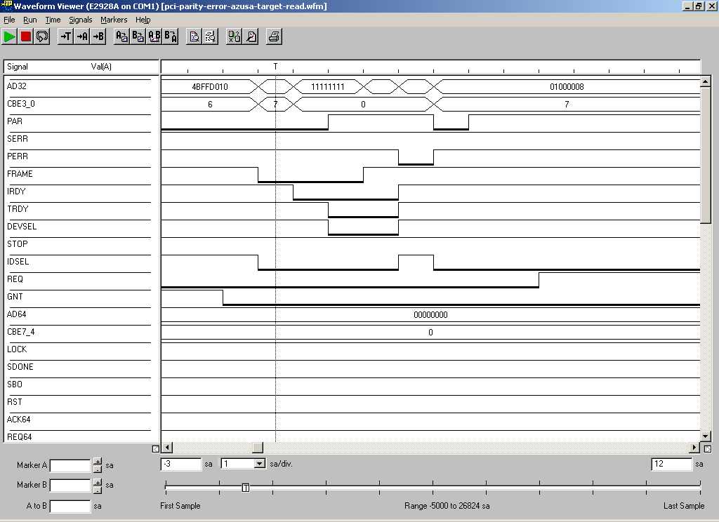
Parity Bit and Perr Timing:
Parity Bit is set one clock cycle after the data is ready, Perr is set two clock cycles after the data is ready to be read. There are two ways to simulate parity error on PCI bus; by triggering the wrong parity bit (Par), or by asserting Perr or Serr signal. On triggering the wrong parity bit, either 1) Azusa acts as initiator and read the data, or 2) Azusa acts as target and PCI master write to it. Agilent PCI tester provides options to set the parity bit PAR to the wrong value.Looking at case 1), example of scipt for Agilent PCI tester as master:
{
   m_xact(busaddr = 1000000\h, cmd = mem_write);
   m_data(data = 11111111\h, dwrpar);
   m_last(data = 8f548f53\h);
}
Here 0x1000000 is the Bar0 address of Azusa PCI controller, "dwrpar "instructs the PCI master to set parity bit to the wrong value, for write trasnfer.The waveform when Azusa acts as target and a PCI tester as Master, writes to it:
And now case 2), example of script for Agilent PCI tester as target:
{
 t_attr(wrpar);
}
Here the "wrpar" instructs the PCI tester to respond with wrong parity bit, for read transfer.The second waveform when Azusa acts as initiator and read from PCI bus:

Type 0 configuration address phase:
PCI CONFIG_ADDRESS register:
We write this format to the PCI CONFIG_ADDRESS register. The enable bit indicates a configuration transaction. For a type 0 config transaction, the PCI controller will generate a PCI address on PCI AD lines based on the diagram below:

Example:

The bits from 31:11 in address word will be matched with IDSEL pin on PCI device.
An example of type 0 address: 0x80000010;
This address will select device with IDSEL pin tied to the AD31 address line. The "1" value in bit 4 will select Bar0 register (offset 4).
An example of type 0 address: 0x00004010;
This address will select device with IDSEL pin tied to the AD14 address line. The "1" value in bit 4 will select Bar0 register (offset 4).
The IDSEL pin is only applicable to type 0 confiuration transaction.
Type 1 configuration address phase:
For type 1 config transaction, the PCI host directly copies the content of the CONFIG_ADDRESS register onto the PCI AD lines during the address phase of a config access.Bus Classification:
There are two kinds of bus: synchronous and asynchronous. In Sync bus, there is a common CLK. For master to initiate request and target to respond, the timing will follow the common CLK. In Async bus, one use req/ack strobing. PCI bus is a sync bus where all transaction happens on the rising edge of the CLK; i.e. device will only "see/check" IRDY and TRDY at the rising edge of the clock. However, it uses IRDY and TRDY to co-ordinate between the master and target.
First created: November 26, 2004
Last Modified: June 14, 2007
Last Modified: June 14, 2007
No comments:
Post a Comment